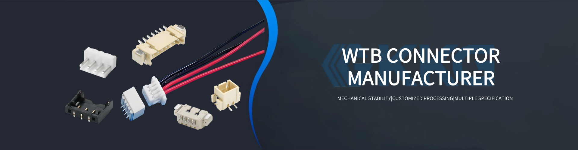

Product Brief Description
Wafer connectors consist of two parts: the base and the terminals. The base is usually made of specialized high-temperature-resistant plastic to withstand high-temperature environments; the terminals are made of conductive metals such as phosphor bronze.
![]() ODM/OEM Service
ODM/OEM Service
![]() Source Factory
Source Factory
![]() Stable Daily Output
Stable Daily Output
![]() High Quality
High Quality
![]() Multiple Payment Methods
Multiple Payment Methods
![]() Pre/After Service
Pre/After Service
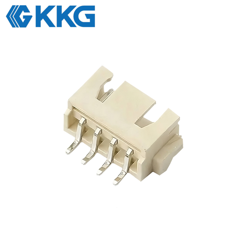
SMD Wafer Connector's Overview
Wafer headers, also known as bases, are connectors mounted on printed circuit boards (PCBs) that typically require soldering to circuit pins. Wafer connectors consist of two parts: the base and the terminals. The base is usually made of specialized high-temperature-resistant plastic to withstand high-temperature environments; the terminals are made of conductive metals such as phosphor bronze, often gold-plated to enhance conductivity and oxidation resistance.
0.8mm wafer connector's Product Structure
1.Contact Design
Material: Contact materials are typically phosphor bronze or brass, with gold plating (thickness ≥0.3μm) to reduce contact resistance (≤20mΩ) and enhance oxidation resistance and wear resistance. For example, Hirose's FX18 series 120P pin sockets feature gold-plated contacts with contact resistance as low as 3mΩ. Structure: Features bellows-type spring design (e.g., TE Connectivity's Free Height series) to withstand insertion/removal abrasion and ensure reliable electrical connection.
2.Insulator
Material: Commonly uses LCP (liquid crystal polymer) or PA66 (nylon 66), with a temperature range of -25°C to +85°C. Some models support -55°C to +105°C (e.g., TE Connectivity series). Protection: Some models feature insulating covers (e.g., TE's Free Height series) to prevent short circuits; pierce-through terminal wire models (e.g., CJT Connectors' 0.8mm wire-to-board connectors) secure wires via the insulator.
3.Positioning and Fixing
Positioning Pins: PCB-side pins (e.g., TE's Free Height series) ensure precise socket placement and prevent soldering misalignment. Polarized Housing: Asymmetric housing design (e.g., Hirose's FX6 series) prevents misalignment and enhances assembly efficiency.
Wafer Pin socket's Working Principle
The operating principle of wafer pin sockets primarily relies on the reliable contact of metal contacts and the circuit conduction mechanism. Combined with structural design, this achieves efficient and stable electrical connections, specifically categorized into the following aspects: Core Operating Mechanism: Metal Contact Engagement and Circuit Conduction Contact Engagement Principle Wafer pin headers establish circuits through direct contact between male (pin) and female (socket) metal contacts. When devices connect, pins insert into the socket's guide slots. Mechanical pressure causes contact surfaces to press tightly together, eliminating gaps and ensuring unimpeded current flow. This design resembles a “closed switch,” providing a low-impedance pathway for signal and power transmission. Signal Transmission Path After contact is made, current flows from the sending device's pins into the socket contacts, then conducts through the female contacts to the receiving device, completing the circuit. Its conductivity depends on the electrical properties of the contact material (e.g., copper alloys), surface plating (e.g., gold plating for oxidation resistance), and contact pressure.
Gold-Plated Wafer Connector's Product Feature
1.Exceptional Corrosion Resistance
The gold plating layer (typically ≥0.3μm thick) provides robust oxidation protection for connector contacts.
2.Low Contact Resistance and High Conductivity
Gold plating significantly reduces contact resistance (≤20mΩ), minimizing signal transmission loss.
3.Enhanced Mechanical Durability
Its wear resistance ensures contacts maintain physical integrity during prolonged use, sustaining stable electrical performance.
4.Superior Thermal Resistance
Gold plating withstands high-temperature environments, preventing performance degradation or material deformation caused by heat.
5.High-Density and Miniaturization Support
Gold-plated contacts enable multi-pin configurations, meeting the demands of miniaturized electronics like smartphones and wearables while preserving signal integrity.
6.Standardization and Modular Advantages
Gold-plated wafer connectors commonly utilize standardized interfaces, supporting modular assembly to shorten device development cycles.

Consumer Electronics
Smartphones, tablets, wearable devices, etc., utilize compact designs to optimize internal space.
Automotive Electronics
In-vehicle displays, battery management systems (BMS), etc., withstand vibration environments and ensure stable connections through locking mechanisms.
Industrial and Medical
Industrial inspection equipment, medical endoscopes, etc., meet waterproof and dustproof requirements (e.g., IP67 rating) and operate in harsh environments.
Home Appliances
Televisions, microwave ovens, rice cookers, electronic scales, and other devices requiring waterproof and dustproof capabilities.
Q:May I get free samples?
A:Sure, 10-20 pcs of free samples are available for normall models. We need to confirm height, operation force and price before shipment.
Q:Can you accept small order, like 1000 pcs , 2000 pcs ?
A:Sure, but we suggest you buy more, because it really can save you time and freight charge in the near future.
Q:How about your quality control?
A:All the products will be 100% checked before the shipment.
Q:Are you a factory or trading company?
A:We are factory, we can provide competitive price.welcome to visit our factory.
Q. Could I have prices of your products?
A.Welcome. Please feel free to send us an email here. You will get our reply in 24 hours
Previous: No
Tel:
Add:
Rixing Industrial Zone,Tangxia Town, Dongguan City, Guangdong Province, China


Copyright © 2025 KKG ELECTRONICS ELECTRIC Co., LTD. All rights reserved
Privacy policy Cookie tracking